Object: Study of Integrator using Operational Amplifier.
Apparatus Required: Bread Board, 741 IC, ±12V supply, Resistors, Capacitor and connecting leads.
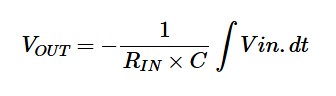
Theory: It is a circuit designed with Op-Amp in such a way that it performs the mathametical Integration operation, its output is proportional to the amplitude and time duration of the input applied. The integrator circuit layout is same as a inverting amplifier but the feedback resistor is replaced by a capacitor which make the circuit frequency dependent. In this case the circuit is derived by the time duration of input applied which results in the charging and discharging of the capacitor. Initially when the voltage is applied to integrator the uncharged capacitor allows maximum current to pass through it and no current flows through the Op-Amp due to the presence of virtual ground, the capacitor starts to charge at the rate of RC time constant and its impedence starts to increase with time and a potential diffrence is develops accross the capacitor resulting in charging current to decrease.This results in the ratio of capacitor’s impedance and input resistance increasing causing a linearly increasing ramp output voltage that continues to increase until the capacitor becomes fully charged.
Output Voltage:
Ciruit Diagram:

Values of Components:
Let C = 0.01µF
Then Ri = 15KΩ
Take Rf = 10Ri = 150KΩ
Procedure:
- Connections are given as per the circuit diagram.
- + Vcc and – Vcc supply is given to the power supply terminal of the Op-Amp IC.
- By adjusting the amplitude and frequency knobs of the function generator, appropriate
input voltage is applied to the inverting input terminal of the Op-Amp. - The output voltage is obtained in the CRO and the input and output voltage waveforms
are plotted in a graph sheet.
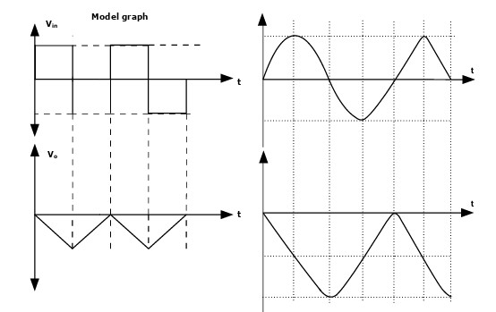
Waveform:
Precautions:
- Add Parallel Resistor
- Use Offset Null
- Use Low-Leakage Capacitor
- Check Voltage Limits
- Connect Power First
- Verify Polarity
Result: The design of the Integrator circuit was done and the input and output waveforms were obtained.